Over the past decade, the development of solar cells has been significantly influenced by semiconductors known as hybrid perovskites. These materials have sparked intense interest within the scientific community due to their ease of processing and the high efficiency they enable under various irradiation conditions. Efficiencies exceeding 24% have been reported in the past year, demonstrating their competitiveness with monocrystalline silicon and thin-film technologies.
Since their emergence in 2009, perovskites have undergone numerous optimizations in device architectures which have been incorporated in other technologies , including solar cells with mesoporous [1] and planar layers [2], as well as multilayer devices known as tandem cells [3]. The concept of using three or four semiconductors with different bandgaps to absorb a broad range of the solar spectrum—from ultraviolet to far-infrared—is not exclusive to multi-junction devices. Tandem architectures with materials of differing properties, known as hybrid tandems, have shown a better efficiency-to-cost ratio compared to III-V multi-junction cells [4]. This is where tandem perovskite cells play a pivotal role. Various configurations have been explored, including thin-film semiconductor cells made of Copper-Indium-Gallium-Selenide (CIGS), Cadmium Telluride (CdTe), organic photovoltaic (OPV) cells, and silicon cells [5,6] (Figure 1a). Among these, textured architectures combining perovskite and monocrystalline silicon heterojunctions (Figure 1b) have demonstrated the highest certified efficiencies for small devices (<1 cm²), achieving 24% in 2017 and 33.9% in 2024 [7]. What configuration has enabled such high efficiencies? Tandem perovskite architectures are divided into three families based on the number of output connections in the photovoltaic device. The most efficient cells to date are known as two-terminal (2T) cells (Figure 2). These devices operate like two cells in series, with their constituent layers fabricated one atop the other on a single substrate. Optimization efforts for these cells have primarily focused on coupling the individual currents of each sub-cell and passivating the interfaces between constituent materials. Other tandem perovskite device options include three-terminal (3T) and four-terminal (4T) architectures, the latter being the easiest to fabricate since each cell can be fabricated separately and then stacked using an encapsulant or adhesive. However, these devices are generally less efficient than 2T cells because radiation can be lost through reflection and/or absorption at the interface between individual cells. For 3T cells, they show the greatest potential for efficiency improvements. Simulations indicate these devices could achieve efficiencies close to 40%, without relying heavily on the bandgap of the perovskite material used [8]. Additionally, complementary studies have focused on designing electrical connections between the cells, paving the way for the production of large-format panels and ensuring their commercial viability in the coming years.
The 2024 year ends not only with record efficiencies on a small scale for tandem cells. Companies like Oxford PV and GCL have demonstrated that tandem perovskite-silicon technology can be industrially manufactured, producing panels of 1.7 m² with certified efficiencies around 27% [9,10]. The next few years will be critical for this technology. Reliability, reproducibility, and stability will be the pillars determining its success and integration into the photovoltaic market, which is simultaneously witnessing the emergence of new, more competitive, and efficient silicon technologies, such as Interdigitated Back Contact (IBC) cells.
Figure 1. a) Certified efficiency values for different families of cells and architectures (certified efficiency values from NREL). b) Typical device structure of a tandem perovskite-silicon cell.
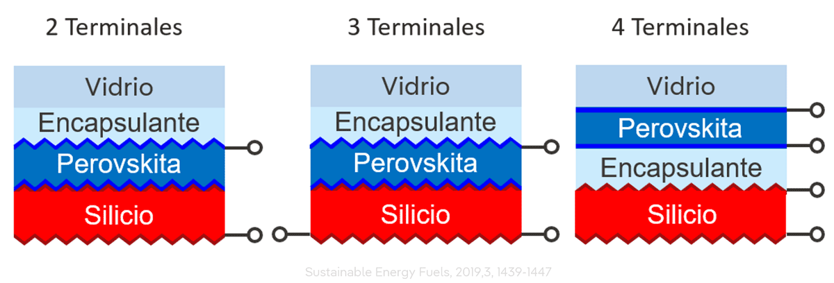
Figure 2. Tandem Perovskite Cell Architectures (Adapted from: Sustainable Energy Fuels, 2019, 3, 1439-1447)
References:
- Zhao, Y., Nardes, A. M., & Zhu, K. (2014). Mesoporous perovskite solar cells: material composition, charge-carrier dynamics, and device characteristics. Faraday discussions, 176, 301-312.
- Tan, H., Jain, A., Voznyy, O., Lan, X., García de Arquer, F. P., Fan, J. Z., … & Sargent, E. H. (2017). Efficient and stable solution-processed planar perovskite solar cells via contact passivation. Science, 355(6326), 722-726.
- Li, H., & Zhang, W. (2020). Perovskite tandem solar cells: from fundamentals to commercial deployment. Chemical Reviews, 120(18), 9835-9950.
- Li, Z., Zhao, Y., Wang, X., Sun, Y., Zhao, Z., Li, Y., … & Chen, Q. (2018). Cost analysis of perovskite tandem photovoltaics. Joule, 2(8), 1559-1572.
- GREEN, Martin A., et al. Solar cell efficiency tables (Version 64). Progress in photovoltaics: research and applications, 2024, vol. 32, no 7, p. 425-441.
- CHU, Qian-Qian, et al. Progress, challenges, and further trends of all perovskites tandem solar cells: A comprehensive review. Materials Today, 2023.
- LIU, Jiang, et al. Perovskite/silicon tandem solar cells with bilayer interface passivation. Nature, 2024, vol. 635, no 8039, p. 596-603.
- GILIBERTI, Gemma; CAGNONI, Matteo; CAPPELLUTI, Federica. Monolithic 3-terminal perovskite/silicon HBT-based tandem compatible with both-side contact silicon cells: a theoretical study. EPJ Photovoltaics, 2023, vol. 14, p. 37.
- GCL says perovskite solar module passes silicon degradation tests. (2024, June 20). Pv Magazine International. https://www.pv-magazine.com/2024/06/20/gcl-says-perovskite-solar-module-passes-silicon-degradation-tests/
- Norman, W. (2024, September 5). Oxford PV ships first commercial perovskite tandem modules. PV Tech. https://www.pv-tech.org/oxford-pv-ships-first-commercial-perovskite-tandem-modules/