The term thin-film solar cell, or second-generation solar cell, refers to a particular type of photovoltaic (PV) device whose main characteristic is the reduced amount of active material required to manufacture efficient cells. Probably best expressed by Ken Zweibel in 2004: “the fundamental idea of thin-film-based PV technology is to use a tiny amount, on the order of a micron thick, of expensive material – the semiconductors that enable the cells to function – and a lot of cheap glass, metal and plastic to complete the PV module”.
The strategy seems reasonable in any manufacturing scenario. But its importance makes perfect sense in contrast to the dominant technology in electronics and photovoltaics, based on silicon wafers of typical thicknesses between 150 and 300 microns. If the determining factor for the expansion of renewable energies (and photovoltaics in particular) is their cost per unit of power that the source in question can generate (€/W), reducing the amount of “expensive” material needed to manufacture efficient solar cells by a factor of, say, 100 compared to conventional technology can have a huge impact on accelerating the development of solar energy, even if such alternative technology does not reach the same levels of efficiency but still retains a favorable €/W ratio. That’s actually the question: achieving favorable €/W ratios from a significant reduction in the numerator. Another intrinsic advantage of this technology also contributes in this direction: while silicon-based module manufacturing involves three consecutive steps (material, cell and module manufacturing), thin-film technologies make it possible to go directly from material to module through what is known as monolithic integration (cells and modules are manufactured simultaneously by means of a subtly designed cell interconnection system).
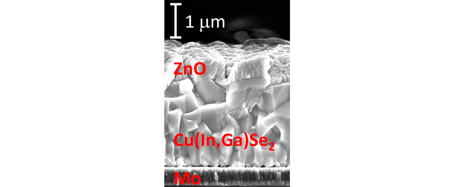
Thin-film solar cells have undergone remarkable development over the past 25 years. Among their various technologies, three of them are currently commercial: amorphous silicon (a-Si), cadmium telluride (CdTe) and copper indium gallium selenide (CIGS)-based chalcopyrites, the latter two with demonstrated efficiencies above 22% and 23%, respectively. Their market share has been reduced, however, due to the extraordinary reduction in costs associated with conventional silicon wafer-based manufacturing, coinciding with the photovoltaic boom of recent years.
Far from abandoning the race, thin-film technologies are still active, improving their processes and researching new materials that allow them to use their characteristic manufacturing architecture (i.e. using little expensive material and a lot of cheap material). The main applications in sight are of two types: designing efficient cells/modules capable of competing with silicon; or alternatively, allying with it, through more sophisticated devices, such as tandem cells, in which the devices actually consist of two (or more) sub-cells. In both cases, a new family of materials, perovskites, used in thin-film devices, seems set to revolutionize the industry.